Join World's Fastest Growing B2B Network
Join World's Fastest Growing B2B Network


| MOQ | 1 set |
| Port | Shanghai |
| Packaging | wooden carton |
| Lead Time | 3-6 months |
| Suitable object | DCB | Object size | Max:190×140mm |
| Sample thickness | 1-2mm | Inspecting Speed | 9.6s/pcs |
| Defect searching method | Image contrast+ logic algorithm | Detectable flaw | short-circuit,connecting line, chipped edge, residual copper, copper deficiency, |
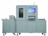
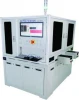
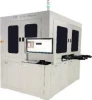
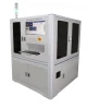
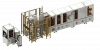
Automatic Ceramic Substrate Defect Inspection Equipment
Function
This AOI equipment is a high-precision offline defect detection equipment for ceramic substrate, which can inspect a size of 140mm*190mm. It can be used to check defects such as chipped ceramic edges, copper surface oxidation, circuit breakage, over corrosion, dint, scratches, surface copper deficiency, dimple, wrinkles, bumps, cutting dislocation, poor plating, poor resistance welding and other defects.
Application
Production and Quality control of ceramic substrates with high quality requirements
Features
1. Combination of multiple high-resolution optical systems ;
2. Lighting design with a variety of LED line light sources;
3. Available with several kinds of marking methods to identify the defect location;
4. Multi-station detection reduces the omission ratio ;
5. Adaptable to certain level of board warp;
6. Data storage function for quality evaluation and process optimization;

Specifications
|
NO |
Item |
Parameter |
|
01 |
Dimension |
1930mm (L) ×1430mm (W) × 1900mm (H) |
|
02 |
Weight |
1500kg |
|
03 |
Power Supply |
AC220V+10% (Single-phase three-wire) |
|
04 |
Air Supply |
6-8kgf/cm2 |
|
05 |
Temperature/ himidity |
17-35℃ / RH<70% |
|
06 |
Power |
Rated 10KW/ Actual 7KW |
|
07 |
Language |
English |
|
Other Parameters |
||
|
NO |
Item |
Parameter |
|
01 |
Suitable object |
DCB |
|
02 |
Object size |
Max:190×140mm; |
|
03 |
Sample thickness |
1-2mm |
|
04 |
CCD Pixel |
AOI 1:13um/Pixel AOI 2/3:24um/Pixel |
|
05 |
Board warp solution |
Auto focus |
|
06 |
CAM format |
Gerber |
|
07 |
Image Processing method |
CCD Color software |
|
08 |
Inspecting Speed |
9.6s/pcs |
|
09 |
Data source |
CAM+graphic scanning |
|
10 |
Auxiliary function |
Laser marking |
|
11 |
Defect Confirmation |
AOI on-line |
|
12 |
Positioning Way of ceramic substrate |
Automatic |
|
13 |
Defect searching method |
Image contrast+ logic algorithm |
|
14 |
Detectable flaw |
AOI 1: short-circuit,connecting line, chipped edge, residual copper, copper deficiency, copper surface stain, copper surface oxidation, cutting dislocation, ink disconnection, ink shedding, ink contamination, reverse resistance welding mark , resistance welding dislocation , resistance welding pinhole ., etc . AOI 2:dint, scratches, wrinkles, bumps; AOI 3:bubble, indentation ; |
One moment please
 Member's Area
 Messages
  Need Help