Join World's Fastest Growing B2B Network
Join World's Fastest Growing B2B Network


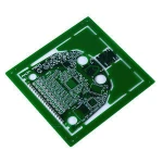
The printed circuit board design is based on the circuit schematic diagram to realize the functions required by the circuit designer. The online PCB design mainly refers to layout design, which needs to consider various factors such as the layout of external connections, the optimal layout of internal electronic components, the optimal layout of metal wiring and through holes, electromagnetic protection, heat dissipation and so on. Excellent layout design can save production costs and achieve good circuit performance and heat dissipation performance. Simple layout design can be implemented manually, and complex layout design needs to be implemented with the aid of computer-aided design (CAD).

An automated software program establishes a convenient method in PCB design that can be easily converted to a physical PCB. Listed below are some popular design tools such as Altium Designer, Eagle, and OrCAD.
Altium Designer is more commonly used in China. This software is relatively simple and the design is more casual. It is not very good to use this software for complex PCBs.
Cadence SPB, the ORCAD schematic design is an international standard; PCB design and simulation are very complete, which is more complicated to use than protel, mainly because the requirements and settings are complicated; Protel is obviously powerful.
Mentor. The current MentorEE version is Mentor EE 7.9. It belongs to the same level of PCB design software as Cadence SPB. It is inferior to cadence SPB in some places. Its strengths are pulling wire and flying wire. It is called a flying wire king.
EAGLE Layout This is the most widely used PCB design software in Europe.
The PCB online design software mentioned above is used a lot, and Cadence SPB and MentorEE are well-deserved kings.

Zuken's CADSTAR PCB design software provides a complete design environment. CADSTAR provides design capabilities throughout the PCB design process, from schematic to layout, routing, signal integrity simulation, power integrity analysis, and 3D mechanical integration.
SPEEDAPCB's senior designers with rich design experience will provide one-to-one PCB design service for you, we can handle many different kinds of PCB circuit design, including high-frequency PCB design. And we will strive to satisfy customers. Reduce the number of R & D and the costs for you.
Design delivery period and capability
| Quantity | Delivery Time(working day) |
| 0-1000PIN | 1-3 days |
| 1000-3000PIN | 3-5 days |
| 3000-5000PIN | 5-7 days |
| 5000-8000PIN | 7-10 days |
| 8000-10000PIN | 10-13 days |
| 10000-20000PIN | 13-20 days |
| Highest layer of HDI | 20 layers |
| Highest level HDI | HDI any level of 24 |
| Highest layer of design | 52 layers |
| Min line width | 2.5mil |
| Min line spacing | 2.5mil |
| Min hole size | 6mil(4mil laser drilling) |
| Min BGA spacing | 0.35mm |
| Max BGA-PIN | 3600PIN |
| Highest speed signal | 28GBPS |
PCB Design Process

PCB Design Tools

One moment please
 Member's Area
 Messages
  Need Help