Join World's Fastest Growing B2B Network
Join World's Fastest Growing B2B Network


Overview
PCB design basics is a basic concept in electronics engineering that refers to the layout and design of printed circuit boards (PCBs). It is the process of creating a plan for how a circuit should be built and laid out on the board. It includes the placement of components, the routing of traces, the design of power supplies, and the selection of materials for the board. The PCB design basics involve understanding the electrical, structural, and thermal requirements of the board, as well as the industry standards and regulations that must be followed. It requires knowledge of the components and the board's manufacturing processes. The PCB design basics also involve ensuring that the board meets all of its performance requirements, such as signal integrity and power delivery. It is important to understand the basics of PCB design in order to create a reliable and cost-effective PCB.
Printed circuit layout Rules
PCB design basics is a basic concept in electronics engineering that refers to the layout and design of printed circuit boards (PCBs). It is the process of creating a plan for how a circuit should be built and laid out on the board. It includes the placement of components, the routing of traces, the design of power supplies, and the selection of materials for the board. The PCB design basics involve understanding the electrical, structural, and thermal requirements of the board, as well as the industry standards and regulations that must be followed. It requires knowledge of the components and the board's manufacturing processes. The PCB design basics also involve ensuring that the board meets all of its performance requirements, such as signal integrity and power delivery. It is important to understand the basics of PCB design in order to create a reliable and cost-effective PCB.
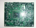
China PCB layout Design Steps
PCB process steps involve several stages, including design, gerber file creation, prototype assembly, mass production, and testing.
The first step is to design a PCB in a software program, taking into account the required PCB size, components, and desired features. This design is then converted into a gerber file, which is used to create a prototype board.
The prototype board is then assembled by assembling components on the board and soldering them into place. This prototype is then tested to ensure it functions as intended. If any issues are found, the design is modified and a new prototype is created.
Once the prototype is approved, the design is used to create the PCBs for mass production. During this stage, the PCBs are fabricated, populated with components, and inspected for defects. The boards are also tested to ensure they meet the desired specifications.
Finally, the PCBs are shipped to the customer and the process is complete.
If you are looking for a reliable pcb layout company , don't hesitate to contact us!
GT, as an excellent best chinese pcb manufacturer, offers a wide range of pcb board assembly for you to choose from.
Room 401,No.5 Building, Dingfeng Technology Park, Shayi Community, Shajing Town, Bao'an District,Shenzhen,Guangdong Province,China
One moment please
 Member's Area
 Messages
  Need Help