Join World's Fastest Growing B2B Network
Join World's Fastest Growing B2B Network


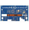
| Model NO. | UC-3852 | Production Process | Subtractive Process |
| Base Material | Copper | Insulation Materials | Epoxy Resin |
| Brand | Uc | Lead Time | 5 Working Days |
| Material Finished Thickness | 1.0mm | Special | Peelable Solder Mask |
| PCB Testing | E-Testing, Flying Probe Testing | Ipc Standards | Ipc Class II |
| Base Material Type | Fr4 | Soldermask Color | Green |
| Surface Finish | Hal Lead Free | Board Layer | 2 |
| Size | 160*180mm | Transport Package | Vacume |
| Specification | UL(US&Canada). ISO9001. RoHs, TS, SGS | Trademark | uc |
| Origin | China | HS Code | 85340090 |
| Production Capacity | 20000 Sqm/Month |
| Files | Gerber, Protel, Powerpcb, Autocad, Cam350, etc |
| Material | FR-4, Hi-Tg FR-4, Lead free Materials (RoHS Compliant) , CEM-3, CEM-1, Aluminium, High frequency Material (Rogers, Teflon, Taconic) |
| Layer No. | 1 - 30 Layers |
| Board thickness | 0.0075"(0.2mm)-0.125"(3.2mm) |
| Board Thickness Tolerance | ±10% |
| Copper thickness | 0.5OZ - 4OZ |
| Impedance Control | ±10% |
| Warpage | 0.075%-1.5% |
| Peelable | 0.012"(0.3mm)-0.02'(0.5mm) |
| Min Trace Width (a) | 0.005"(0.125mm) |
| Min Space Width (b) | 0.005"(0.125mm) |
| Min Annular Ring | 0.005"(0.125mm) |
| SMD Pitch (a) | 0.012"(0.3mm) |
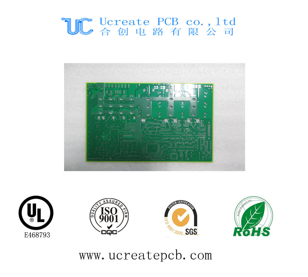
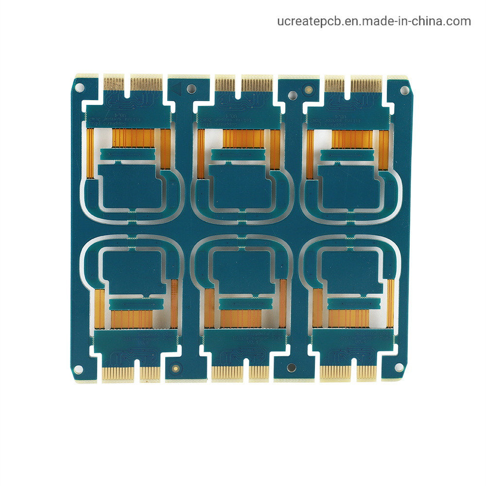
| pcb with green solder mask and LF-FREE surface finishing BGA Pitch (b) | 0.027"(0.675mm) |
| Regesiter torlerance | 0.05mm |
| Min Solder Mask Dam (a) | 0.005"(0.125mm) |
| Soldermask Clearance (b) | 0.005"(0.125mm) |
| Min SMT Pad spacing (c) | 0.004"(0.1mm) |
| Solder Mask Thickness | 0.0007"(0.018mm) |
| Hole size | 0.01"(0.25mm)-- 0.257"(6.5mm) |
| Hole Size Tol (+/-) | ±0.003"(±0.0762mm) |
| Aspect Ratio | 6:01 |
| Hole Registration | 0.004"(0.1mm) |
| HASL | 2.5um |
| Lead free HASL | 2.5um |
| Immersion Gold | Nickel 3-7um Au:1-3u'' |
| OSP | 0.2-0.5um |
| Panel Outline Tol (+/-) | ±0.004''(±0.1mm) |
| Beveling | 30°45° |
| V-cut | 15° 30° 45° 60° |
| Surface finish | HAL, HASL Lead Free, Immersion gold, Gold plating, Gold finger, immersion silver, immersion Tin, OSP, Carbon ink, |
| Certificate | ROHS ISO9001:2000 TS16949 SGS UL |
| Special requirements | Buried and blind vias, Impedance control, via plug, BGA soldering and gold finger |


One moment please
 Member's Area
 Messages
  Need Help