Join World's Fastest Growing B2B Network
Join World's Fastest Growing B2B Network


| MOQ | 1 pcs |
| Port | SHENZHEN |
| Packaging | Customer settings |
| Lead Time | 5-30days |
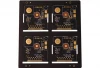
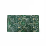
Fast supply electric circuit board assembly manufacturer
4 YAMAHA High-speed SMT Lines
6 million daily SMT placements capability
400,000 daily DIP placements capability
500×600 mm Maximum Board Size
0.25"x 0.25" Minimum Board Size
450 mm Max. Width for Wave-Solder
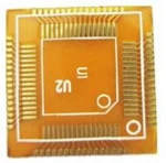
Passives Components Down to 0201 Size BGA and VFBGA Leadless Chip Carrier/CSP Double-Sided SMT Assembly Fine Pitch to 08 Mil BGA Repair and ReballPart Removal and Replacement
SMT and DIP/X-RAY Inspection/AOI Testing/In-circuit-test (ICT)/Flying Probe/Function Test/Burn-in/Finished products assembly
What is a DHI board?
High Density Interconnector (HDI), is a circuit board with a relatively high density of line distribution using micro-bumping. The HDI PCB assembly manufacturing has an inner layer line and an outer layer line, and uses a process such as drilling and metallization in the hole to connect the inside of each layer. HDI boards are generally manufactured by a laminated method. The more times the layers are stacked, the higher technical grade of the board is. The common HDI boards are basically one-time laminated, high-grade HDI uses two or more layers of technology. Meanwhile it adopts advanced PCB technology such as stacking holes, plating holes, and laser direct drilling to finish.
Advantages of the HDI board
1. When the density of the PCB increases beyond the eight-layer board, the cost will be lower than the conventional complicated pressing process if manufactured by HDI board.
2. The electrical performance and signal correctness of HDI board are higher than traditional PCB.
3. HDI board has better improvement for radio frequency interference, electromagnetic wave interference, electrostatic discharge and heat conduction.
4. The most common reason for using HDI technology is a significant increase in packaging density. The space obtained by the finer track structure can be used for components.
5. Reducing overall space requirements will result in smaller board sizes and fewer layers.
Electronic products continue to develop toward high density and high precision. The so-called "high", not only refer to improve machine performance, but also reduces the size of the machine. High-density integration (HDI) technology enables the design of end-product to be more compact while meeting higher standards of electronic performance and efficiency. Currently, many popular electronic products, such as mobile phones, medical devices, notebook computers, automotive electronics, etc., are mostly using HDI boards. With the upgrading of electronic products and the needs of the market, the development of HDI boards will be very rapid.
We're capable of manufacturing HDI PCB up to 20 layers in various structures.
Check our HDI PCB capabilities by below table:
|
Feature |
Capability |
|
Quality Grade |
Standard IPC 2 |
|
Number of Layers |
2 - 20layers |
|
Build Time |
2days - 5weeks |
|
Material |
FR4 standard Tg 140°C,FR4 High Tg 170°C, FR4 and Rogers combined lamination |
|
Board Size |
Max 500*600mm |
|
Board Thickness |
0.25mm - 5.0mm |
|
Copper Weight (Finished) |
0.5oz - 6.0oz |
|
Min Tracing/Spacing |
3mil/2.8mil |
|
Solder Mask Color |
Green, White, Blue, Black, Red, Yellow |
|
Silkscreen Color |
White, Black, Yellow |
|
Surface Finish |
HASL - Hot Air Solder Leveling |
|
Lead Free HASL - RoHS |
|
|
ENIG - Electroless Nickle/Immersion Gold - RoHS |
|
|
Immersion Silver - RoHS |
|
|
Immersion Tin - RoHS |
|
|
OSP - Organic Solderability Preservatives - RoHS |
|
|
Min Annular Ring |
4mil, 3mil - laser drill |
|
Min Drilling Hole Diameter |
6mil, 4mil - laser drill |
|
Other Techniques |
Flex-rigid combination |
|
Via In Pad |
|
|
Buried Capacitor (only for Prototype PCB total area ≤1m²) |
Discuss your HDI printed circuit board today? You can click right side button contact us for a detailed quote.
5th Floor, Building F, Hongfa Technology Industrial Park, Tangtou Community, Shiyan Street, Baoan District
One moment please
 Member's Area
 Messages
  Need Help