Join World's Fastest Growing B2B Network
Join World's Fastest Growing B2B Network


| MOQ | 1 piece |
| Port | china |
| Lead Time | 2to3days |
https://www.wallystech.com/products_show.php?id=53&lm=1
email:[email protected]
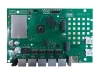
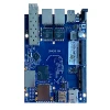
Featuring withindustrial-grade IPQ4019 chipset
Integrated with 2x 2 5G high power
Radio module and 2x2 2.4G high power Radio module
Support 5.180GHz to5.825GHz Frequency Range;
Support 2.412GHz to 2.482GHz
Support 2 x 5G MMCX Connectors and 2x2.4G MMCX
20MHz/40MHz/80MHz Bandwidth
Support 11ABGN/AC
RoHS compliance ensure a high level
protection of human health and the environment from risks that can be posed by
|
Absolute Maximum Rating |
|
Parameter |
Rating |
Unit |
|
Supply Voltage |
24V~48 |
V |
|
Operating Temperature Range |
-40 to +70 |
ºC |
|
Storage Temperature Range |
-45 to +105 |
ºC |
|
Operating Humidity Range |
5 to +95 (non-condensing) |
% |
|
Storage Humidity Range |
0 to +90 (non-condensing) |
% |
| Hardware Specifications |
|
Symbol |
Parameter |
|
CPU |
IPQ4019(Quad core ARM Cortex A7 at 716.8 MHz) |
|
Antenna Connector |
2 x 5G MMCX connectors;2x2.4G MMCX |
|
10/100/1000Mbps |
2xRJ45 |
|
DC Jack |
12 power supply |
|
ROHS Compliance |
YES |
|
Dimension |
65mmx35mm x 16mm |
|
Max Power |
12V x 0.8A= 9.6W |
|
Nor Flash |
32MB |
|
DDR |
256MB |
|
Radio TX Specifications(5180MHz-5825MHz) |
|
Operating Mode |
Data Rate |
Power |
Tolerance |
|
|
1 Chain |
2 Chains |
|||
|
802.11a |
6 Mbps |
26dBm |
29dbm |
±2dB |
|
54 Mbps |
22dBm |
25dbm |
±2dB |
|
|
802.11n HT20 |
MCS0, MCS8 |
26dBm |
29dbm |
±2dB |
|
MCS7, MCS15 |
22dBm |
25dbm |
±2dB |
|
|
802.11n HT40 |
MCS0, MCS8 |
25dBm |
28dbm |
±2dB |
|
MCS7, MCS15 |
21dBm |
24dbm |
±2dB |
|
|
802.11ac |
MCS0, MCS10,MCS20 |
25dBm |
28dbm |
±2dB |
|
MCS9,MCS19,MCS29 |
19dBm |
22dbm |
±2dB |
|
|
Radio RX Specifications(5180MHz-5825MHz)
|
|
Operating Mode |
Data Rate |
Sensitivity |
|
802.11a |
6 Mbps |
-92dBm |
|
54 Mbps |
-74dBm |
|
|
802.11n HT20 |
MCS0, MCS8 |
-91dBm |
|
MCS7, MCS15 |
-72dBm |
|
|
802.11n HT40
|
MCS0, MCS8 |
-90dBm |
|
MCS7, MCS15 |
-70dBm |
|
|
802.11AC HT40
|
MCS0, MCS10,MCS20 |
-90dBm |
|
MCS9,MCS19,MCS29 |
-67dBm |
|
|
802.11AC HT80
|
MCS0, MCS10,MCS20 |
-88dBm |
|
MCS9,MCS19,MCS29 |
-62dBm |
|
Radio TX Specifications(2412MHz-2482MHz)
|
|
Operating Mode
|
Data Rate
|
Power |
Tolerance
|
|
|
1 Chain |
2 Chains |
|||
|
802.11g |
6 Mbps |
25dbm |
28dbm |
±2dB |
|
54 Mbps |
22dbm |
25dbm |
±2dB |
|
|
802.11n HT20 |
MCS0, MCS8 |
25dbm |
28dbm |
±2dB |
|
MCS7, MCS15 |
21dbm |
24dbm |
±2dB |
|
|
802.11n HT40 |
MCS0, MCS8 |
25dbm |
28dbm |
±2dB |
|
MCS7, MCS15 |
21dbm |
24dbm |
±2dB |
|
|
Radio RX Specifications(2412MHz-2482MHz) |
|
Operating Mode |
Data Rate |
Sensitivity |
|
802.11g |
6 Mbps |
-91dBm |
|
54 Mbps |
-73dBm |
|
|
802.11n HT20 |
MCS0, MCS8 |
-90dBm |
|
MCS7, MCS15 |
-72dBm |
|
|
802.11n HT40 |
MCS0, MCS8 |
-90dBm |
|
MCS7, MCS15 |
-70dBm |
| Pin Define |

|
Pin number |
signal |
Pin number |
signal |
Pin number |
signal |
|
1 |
GND |
36 |
GND |
54 |
GND |
|
2 |
GND |
37 |
GND |
55 |
P4_TRX2+ |
|
3 |
GND |
38 |
GND |
56 |
P4_TRX2- |
|
4 |
GND |
39 |
GND |
57 |
P4_TRX3+ |
|
5 |
GND |
40 |
GND |
58 |
P4_TRX3- |
|
6 |
GND |
41 |
P3_TRX0+ |
59 |
GND |
|
7 |
GND |
42 |
P3_TRX0- |
60 |
P4_1000_LED |
|
8 |
GND |
43 |
P3_TRX1+ |
61 |
2G_LINK_LED_1P8 |
|
9 |
GND |
44 |
P3_TRX1- |
62 |
GND |
|
10 |
GND |
45 |
P3_TRX2+ |
63 |
GND |
|
11 |
GND |
46 |
P3_TRX2- |
64 |
USB3_SS_TX_P |
|
12 |
GND |
47 |
P3_TRX3+ |
65 |
USB3_SS_TX_N |
|
13 |
GND |
48 |
P3_TRX3- |
66 |
USB3_SS_RX_P |
|
14 |
GND |
49 |
P4_TRX0+ |
67 |
USB3_SS_RX_N |
|
15 |
GND |
50 |
P4_TRX0- |
68 |
USB3_HS_DP |
|
16 |
GND |
51 |
P4_TRX1+ |
69 |
USB3_HS_DM |
|
17 |
GND |
52 |
P4_TRX1- |
70 |
GND |
|
18 |
GND |
53 |
GND |
71 |
2G_STRENGTH_LED |
|
19 |
GND |
|
|
72 |
GND |
|
20 |
GND |
|
|
73 |
GND |
|
21 |
GND |
|
|
74 |
GND |
|
22 |
GND |
|
|
75 |
GND |
|
23 |
GND |
|
|
76 |
GND |
|
24 |
GND |
|
|
77 |
GND |
|
25 |
GND |
|
|
78 |
GND |
|
26 |
GND |
|
|
79 |
12V |
|
27 |
GND |
|
|
80 |
12V |
|
28 |
GND |
|
|
81 |
GND |
|
29 |
GND |
|
|
82 |
GND |
|
30 |
software reset |
|
|
83 |
GND |
|
31 |
GND |
|
|
84 |
GND |
|
32 |
3.3V |
|
|
85 |
GND |
|
33 |
Uart TX |
|
|
86 |
GND |
|
34 |
Uart RX |
|
|
87 |
GND |
|
35 |
GND |
|
|
88 |
GND |
Note:
1) Pin41-Pin48 indicates the differential signals of network port 1, which are 0,1,2, and 3 in sequence
2) Pin48 to Pin52, P55 to Pin58 indicates the differential signals of network port 2. The sequence is differential signals 0,1,2, and 3
The schematic diagram of the extended circuit is as follows:

3) Pin64-Pin69 indicates the differential signals of USB3.0 are TX, RX, and HS in sequence
The schematic diagram of the extended circuit is as follows:

4) Pin 79,80 is a 12V input power signal and the input voltage is in the range of 11v-13v
5) Pin32 -Pin35 indicates the serial port signal, Pin32 indicates the output 3.3V, Pin33, and Pin34 indicates the output input signal
The schematic diagram of the extended circuit is as follows,


One moment please
 Member's Area
 Messages
  Need Help