Join World's Fastest Growing B2B Network
Join World's Fastest Growing B2B Network


| MOQ | 1 piece |
| Packaging | vacumm packing |
| Lead Time | 2-3 weeks |
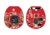
Supplier: Shenzhen Big Electronic Layer Statistics: 8 Application Areas: Measuring Equipment Manufacturer, Procurement, Assembly Circuit Board Assembly Services
PCB parameters: DB2/HP-150 Thickness: 5.5mm Surface treatment (such as testing: 100% electronic testing Packaging: vacuum packaging Delivery time: 10-15 days)
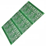
PCB production capacity
Number of layers: 1-30 layers
Quantity: 25,000 square meters per month
PC type: 5OZ immersed copper, impedance board, HDI, high frequency board, aluminum, FPC, soft and hard board circuit board
Basic material brand
High frequency: Rogers, Tacony
HTG: S1000-2M, Lianmao IT180A
Welding mask: Taiyue PSR-2000/4000 series
Surface treatment: HASL, IMU, OSP, IM tin, IM silver, 50-inch hybrid hard plating
Surface treatment: I use gold fingers + OSP I use gold fingers I use silver fingers + gold fingers
Polychlorinated biphenyls technical parameters
Minimum trace width/spacing: 2.5/2.5mil external, 3/3mil internal (1/3, 1/2oz)
Minimum pass: 0.5mm/0.1mm (laser)
Lowest loop: 4 miles
Maximum copper thickness: 7 ounces
Maximum size:650x1100mm
Thickness to aperture ratio: 20:1
tolerate
PTH only: +/-0.0075mm (Simple: +/-0.05mm)
: +/-0.1mm (simple: +/-0.05-0.075mm).
---------------------------------------
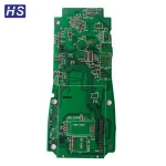
Supplier: Shenzhen Big Electronic Layer Statistics: 8 Application Areas: Measuring Equipment Manufacturer, Procurement, Assembly Circuit Board Assembly Services
PCB parameters: DB2/HP-150 Thickness: 5.5mm Surface treatment (such as test: 100% electronic test Packaging: vacuum packaging Delivery time: 10-15 days)
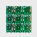
Number of PCB
capacity
layers:
1-30
Quantity:
25,000 square
meters/month
PCB type: 5oz
immersed copper, impedance board, HDI, HF board, aluminum, FPC,
soft-hard board PCB
basic material
brand
HF: Rogers,
Taconic
HTG: S1000 -
2M, Lianmao IT180A
solder mask:
Taiyo PSR-2000/4000
series
surface
treatment: HASL, Im Au, OSP, Im Sn, Im Ag, 50” hard gold plating
mixed
surface
treatment: Im Au+OSP, Im Au+gold Finger, Im Ag+Gold
Finger
PCB Technical
Parameters
Minimum trace
width/size: outer 2.5/2.5mil, inner 3/3mil (1/3,
1/2oz)
minimum via:
0.15mm/0.1mm (laser)
minimum Ring
Ring: 4mil
Maximum Copper
Thickness: 7oz
Maximum Size:
650x1100mm
Thickness
Aperture Ratio: 20:1
Tolerance
PTH only: +/-0.0075mm (Simple: +/-0.05mm)
: +/-0.1mm (Simple: +/-0.05-0.075mm.
Room A510-512 Car Building, No.45 Zhenhua Road,, Futian District, Shenzhen, China 518031
One moment please
 Member's Area
 Messages
  Need Help